Product Features
Core
• Ultra-high speed 8051 core with single clock per machine cycle, which is called 1T and is about 12 times faster than traditional 8051
• Fully compatible instruction set with traditional 8051
• 16 interrupt sources and 4 interrupt priority levels
• Online debugging is supported
Operating voltage
• 1.9 to 5.5V
• Built-in LDO
Operating temperature
• -40°C~85°C
Flash memory
• Up to 17K bytes of Flash memory to be used to store user code
• Configurable EEPROM size, 512bytes single page erased, can be repeatedly erased more than 100 thousand times.
• In-System-Programming, ISP in short, can be used to update the application code, no need for programmer.
• Online debugging with single chip is supported, and no emulator is needed. The number of breakpoints is unlimited theoretically.
SRAM
• 128 bytes internal direct access RAM
• 128 bytes internal indirect access RAM
• 1024 bytes internal extended RAM
Clock
• Internal high precise R/C clock (IRC, range from 4MHz to 36MHz), adjustable while ISP and can be divided to lower frequency by user software, 100KHz for instance
– Error:±0.3 percent (at the temperature 25℃)
– -1.38 percent~+1.42 percent temperature drift (at the temperature range of -40°C to +85°C)
– -0.88 percent~+1.05 percent temperature drift (at the temperature range of -20℃ to 65℃)
• Internal 32KHz low speed IRC with large error
• External 4MHz~33MHz oscillator or external clock
• The three clock source above can be selected freely by used code.
Reset
• Hardware reset
– Power-on reset. Measured voltage value is 1.69V~1.82V. (Effective when the chip does not enable the low voltage reset function) The power-on reset voltage is a voltage range consisting of an upper limit voltage and a lower limit voltage. When the operating voltage drops from 5V / 3.3V to the lower limit threshold voltage of the power-on reset, the chip is in reset state. When the voltage rises from 0V to the upper threshold voltage of power-on reset, the chip is released from the reset state.
– Reset by reset pin. The default function of P5.4 is I/O port. P5.4 pin can be set as the reset pin while ISP download. (Note: When the P5.4 pin is set as the reset pin, the reset level is low.)
– Watch dog timer reset
– Low voltage detection reset. 4 low voltage detection levels are provided, 2.2V (Measured as 1.90V~2.04V), 2.4V (Measured as 2.30V~2.50V), V2.7 (Measured as 2.61V~2.82V), V3.0 (Measured as 2.90V~3.13V). Each level of low-voltage detection voltage is a voltage range consisting of an upper limit voltage and a lower limit voltage. When the operating voltage drops from 5V / 3.3V to the lower limit threshold voltage of low-voltage detection, the low-voltage detection takes effect. When the voltage rises from 0V to the upper threshold voltage, the low voltage detection becomes effective.
• Software reset
– Writing the reset trigger register using software
Interrupts
• 16 interrupt sources: INT0, INT1, INT2, INT3, INT4, timer0, timer1, timer2, uart1, uart2, ADC, LVD, SPI, I2C, comparator,PCA/CCP/PWM
• 4 interrupt priority levels
• Interrupts that can awaken the CPU in clock stop mode: INT0 (P3.2), INT1 (P3.3), INT2 (P3.6), INT3 (P3.7), INT4 (P3.0), T0 (P3.4) ), T1(P3.5), T2(P1.2), RXD(P3.0/P3.6/P1.6), RXD2(P1.4), CCP0(P1.1/P3.5), CCP1 (P1.0/P3.6), CCP2 (P3.7), I2C_SDA (P1.4/P3.3) and comparator interrupt, low-voltage detection interrupt, power-down wake-up timer.
Digital peripherals
• 3 16-bit timers: timer0, timer1, timer2, where the mode 3 of timer 0 has the Non Maskable Interrupt (NMI in short) function. Mode 0 of timer 0 and timer 1 is 16-bit Auto-reload mode.
• 2 high speed UARTs: uart1, uart2, whose baud rate clock source may be fast as FOSC/4
• 3 groups of PCAs: CCP0, CCP1, CCP2, which can be used as capture, high speed output and 6-bits, 7-bits, 8-bits or 10-bits PWM.
• SPI: Master mode, slave mode or master/slave automatic switch mode are supported.
• I2C: Master mode or slave mode are supported.
• MDU16: Hardware 16-bit Multiplier and Divider which supports 32-bit divided by 16-bit, 16-bit divided by 16-bit, 16-bit by 16-bit, data shift, and data normalization operations.
Analog peripherals
• 6 channels (channel 0 to channel 5) ultra-high speed ADC which supports 10-bit precision analog-to-digital conversion, the speed can be as fast as 500K(500,000 conversions per second).
• ADC channel 15 is used to test the internal reference voltage. (The default internal reference voltage is 1.19V when the chip is shipped)
• DAC. 3 groups of PCAs can be used as DAC.
GPIO
• Up to 18 GPIOs: P1.0~P1.7, P3.0~P3.7, P5.4~P5.5
• 4 modes for all GPIOs: quasi-bidirectional mode, push-pull output mode, open drain mode, high-impedance input mode
• Except for P3.0 and P3.1, all other I/O ports are in high-impedance state after power-on. User must set the I/O ports mode before using them. In addition, each I/O can independently enable the internal 4K pull-up resistor.
Package
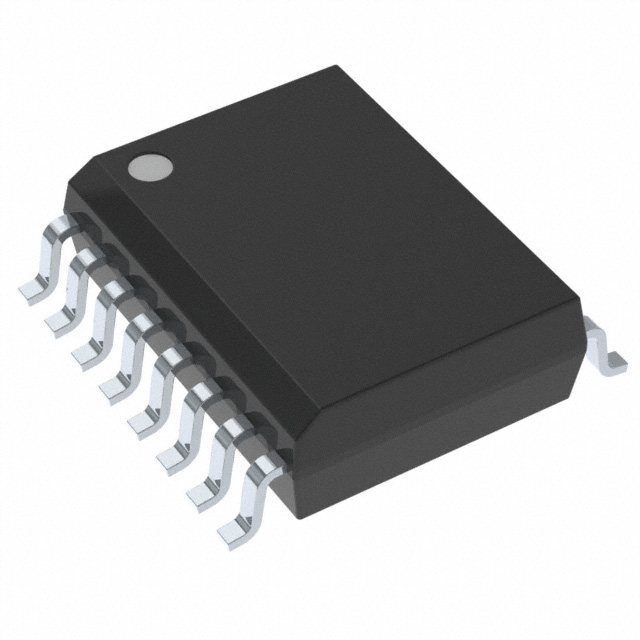
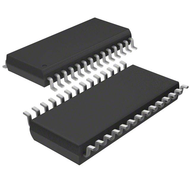
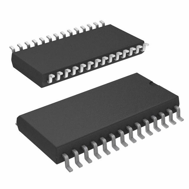
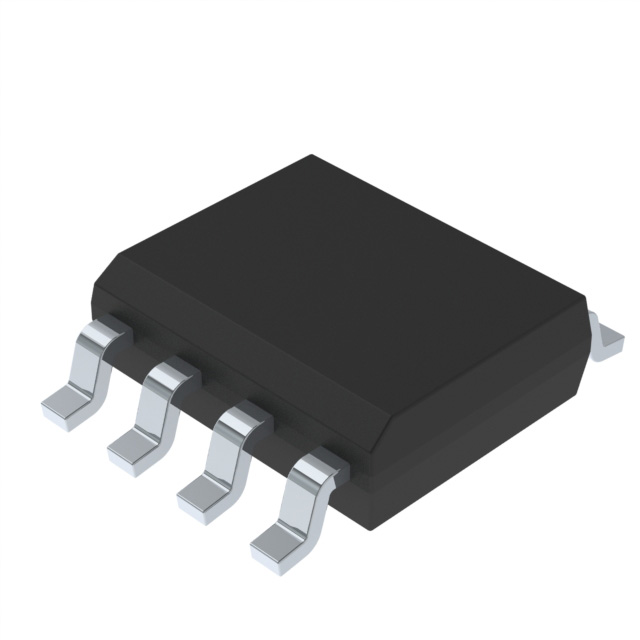
• TSSOP20,QFN20, SOP16,SOP8, DFN8
Specifications
| Part# | STC8G1K08 |
| Type: | MCU microcontroller |
| Manufactor | STC |
| DC | NEW |
| Describe | SOP8 |
| Supplier Device Packaging | REEL |
Actual product photos

Payment&Transportation

Official Certificate&Certificate

Multiple product supply

Company office environment

Warehouse Real Shot

Standard packaging

We also provide :
| Part No | Manufacturer | Date Code | Quantity | Description |
| LM22676ADJ | NS | 19+ | 250 | SOP8 |
| TPS562201DDCR | TI | 22+ | 795500 | SOT23-6 |
| NJG1806K75 | JRC | 22+ | 500000 | DFN6 |
| TLV74318PDQNR | TI | 22+ | 402000 | X2SON-4 |
| NJG1801K75 | JRC | 22+ | 300000 | SMD |
| NJG1804K64 | JRC | 22+ | 300000 | DFN8 |
| LM27761DSGR | TI | 22+ | 151000 | WSON8 |
| TLV62565DBVR | TI | 22+ | 138000 | SOT23-5 |
| TPS613222ADBVR | TI | 22+ | 108000 | SOT23-5 |
| LNK625DG-TL | POWER | 22+ | 100000 | SOP-8 |
| OPA4322AIPWR | TI | 22+ | 100000 | TSSOP14 |
| TLV75528PDRVR | TI | 22+ | 99000 | WSON-6 |
| TPS7A2025PDQNR | TI | 22+ | 78500 | X2SON-4 |
| TLV62568DBVR | TI | 22+ | 72000 | SOT23-5 |
| STM32L051K8U6TR | ST | 22+ | 60000 | QFN32 |
| SKY66421-11 | SKYWORKS | 22+ | 56500 | QFN16 |
| TPS7A1111PDRVR | TI | 22+ | 54000 | WSON6 |
| TLV62569PDDCR | TI | 22+ | 52000 | SOT23-6 |
| TLV62569DBVR | TI | 22+ | 48000 | SOT23-5 |
| TPS23753APWR | TI | 22+ | 40000 | TSSOP14 |
| NB691GG-Z | MPS | 22+ | 30000 | QFN |
| SN74AHC1G02DBVR | TI | 22+ | 27939 | SOT-23 |
| TPS63000DRCR | TI | 22+ | 23238 | VSON10 |
| TLV75533PDRVR | TI | 22+ | 21500 | WSON6 |
| NB687BGQ-Z | MPS | 22+ | 20000 | QFN |
| A3916GESTR-T-1 | ALLEGRO | 22+ | 17150 | QFN-20 |
| TPS62135RGXR | TI | 22+ | 15000 | VQFN11 |
| TLE2022AMDR | TI | 0803+ | 12500 | SOP8 |
| TPS23756PWPR | TI | 22+ | 12000 | HTSSOP-20 |