Product Descriptions
The AT26F004 is a serial interface Flash memory device designed for use in a wide variety of high-volume consumer based applications in which program code is shadowed from Flash memory into embedded or external RAM for execution. The flexible erase architecture of the AT26F004, with its erase granularity as small as 4 Kbytes,makes it ideal for data storage as well, eliminating the need for additional data storage EEPROM devices.
The physical sectoring and the erase block sizes of the AT26F004 have been optimized to meet the needs of today's code and data storage applications. By optimizing the size of the physical sectors and erase blocks, the memory space can be used much more efficiently. Because certain code modules and data storage segments must reside by themselves in their own protected sectors, the wasted and unused memory space that occurs with large sectored and large block erase Flash memory devices can be greatly reduced. This increased memory space efficiency allows additional code routines and data storage segments to be added while still maintaining the same overall device density.
The AT26F004 also offers a sophisticated method for protecting individual sectors against erroneous or malicious program and erase operations. By providing the ability to individually protect and unprotect sectors, a system can unprotect a specific sector to modify its contents while keeping the remaining sectors of the memory array securely protected. This is useful in applications where program code is patched or updated on a subroutine or module basis, or in applications where data storage segments need to be modified without running the risk of errant modifications to the program code segments.
Specifically designed for use in 3-volt systems, the AT26F004 supports read, program, and erase operations with a supply voltage range of 2.7V to 3.6V. No separate voltage is required for programming and erasing.
Product Features
• Single 2.7V - 3.6V Supply
• Serial Peripheral Interface (SPI) Compatible
– Supports SPI Modes 0 and 3
• 33 MHz Maximum Clock Frequency
• Flexible, Uniform Erase Architecture
– 4-Kbyte Blocks
– 32-Kbyte Blocks
– 64-Kbyte Blocks
– Full Chip Erase
• Optimized Physical Sectoring for Code Shadowing and Code + Data Storage Applications
– One 16-Kbyte Top Boot Sector
– Two 8-Kbyte Sectors
– One 32-Kbyte Sector
– Seven 64-Kbyte Sectors
• Individual Sector Protection for Program/Erase Protection
• Hardware Controlled Locking of Protected Sectors
• Byte Program Architecture with Sequential Byte Program Mode Capability
– Sequential Byte Program Mode Improves Throughput for Programming Multiple Bytes
• JEDEC Standard Manufacturer and Device ID Read Methodology
• Low Power Dissipation
– 7 mA Active Read Current (Typical)
– 15 µA Deep Power-down Current (Typical)
• Endurance: 100,000 Program/Erase Cycles
• Data Retention: 20 Years
• Complies with Full Industrial Temperature Range
• Industry Standard Green (Pb/Halide-free/RoHS Compliant) Package Options
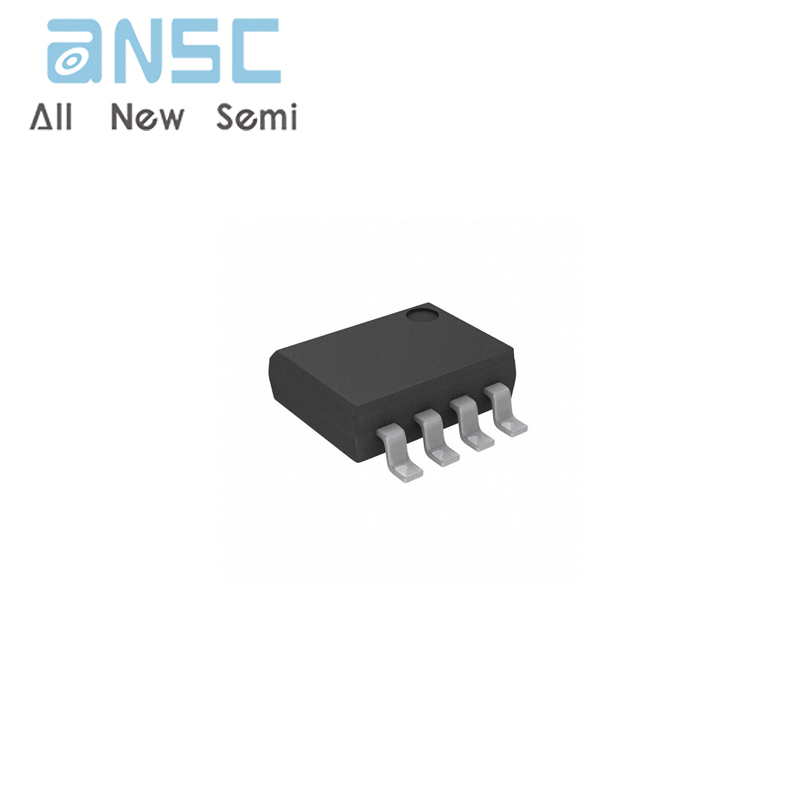
– 8-lead SOIC
– 8-lead MLF
Product Specifications
| Attribute | Attribute value |
| ANSM-Part# | ANSM-AT26F004-SSU |
| Category | Integrated Circuits (ICs) |
| Memory | |
| Memory | |
| Mfr | - |
| Series | - |
| Packaging | Tube |
| Part Status | Obsolete |
| DigiKey Programmable | Not Verified |
| Memory Type | Non-Volatile |
| Memory Format | FLASH |
| Technology | FLASH |
| Memory Size | 4Mbit |
| Memory Organization | 256 Bytes x 2048 pages |
| Memory Interface | SPI |
| Clock Frequency | 33 MHz |
| Write Cycle Time - Word, Page | 5ms |
| Voltage - Supply | 2.7V ~ 3.6V |
| Operating Temperature | -40°C ~ 85°C (TC) |
| Mounting Type | Surface Mount |
| Package / Case | 8-SOIC (0.154", 3.90mm Width) |
| Supplier Device Package | 8-SOIC |
| Base Product Number | AT26F004 |
Product photos

For more product information, please download the PDF