Product Descriptions
The FPGA family delivers high-performance, high-capacity programmable logic solutions. Dramatic increases in silicon efficiency result from optimizing the new architecture for place-and-route efficiency and exploiting an aggressive 5-layer-metal 0.22 μm CMOS process. These advances make FPGAs powerful and flexible alternatives to mask-programmed gate arrays.
Building on experience gained from previous generations of FPGAs, the family represents a revolutionary step forward in programmable logic design. Combining a wide variety of programmable system features, a rich hierarchy of fast, flexible interconnect resources, and advanced process technology, the family delivers a high-speed and high-capacity programmable logic solution that enhances design flexibility while reducing time-to-market.
Product Features
• Fast, high-density Field Programmable Gate Arrays
- Densities from 50k to 1M system gates
- System performance up to 200 MHz
- 66-MHz PCI Compliant
- Hot-swappable for Compact PCI
• Multi-standard SelectIO™ interfaces
- 16 high-performance interface standards
- Connects directly to ZBTRAM devices
• Built-in clock-management circuitry
- Four dedicated delay-locked loops (DLLs) for advanced clock control
- Four primary low-skew global clock distribution nets, plus 24 secondary local clock nets
• Hierarchical memory system
- LUTs configurable as 16-bit RAM, 32-bit RAM, 16-bit dual-ported RAM, or 16-bit Shift Register
- Configurable synchronous dual-ported 4k-bit RAMs
- Fast interfaces to external high-performance RAMs
• Flexible architecture that balances speed and density
- Dedicated carry logic for high-speed arithmetic
- Dedicated multiplier support
- Cascade chain for wide-input functions
- Abundant registers/latches with clock enable, and dual synchronous/asynchronous set and reset
- Internal 3-state bussing
- IEEE 1149.1 boundary-scan logic
- Die-temperature sensor diode
• Supported by FPGA Foundation™ and Alliance Development Systems
- Complete support for Unified Libraries, Relationally Placed Macros, and Design Manager
- Wide selection of PC and workstation platforms
• SRAM-based in-system configuration
- Unlimited re-programmability
- Four programming modes
• 0.22 μm 5-layer metal process
• 100 PERCENT factory tested
Product Specifications
| Attribute | Attribute value |
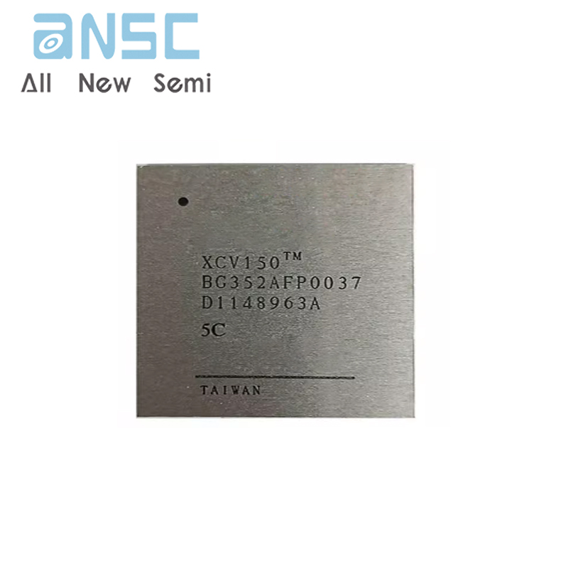
| ANSM-Part# | ANSM-XCV150-5BG352C |
| Category | Integrated Circuits (ICs) |
| Embedded | |
| FPGAs (Field Programmable Gate Array) | |
| Mfr | - |
| Series | Virtex® |
| Packaging | Tray |
| Part Status | Obsolete |
| DigiKey Programmable | Not Verified |
| Number of LABs/CLBs | 864 |
| Number of Logic Elements/Cells | 3888 |
| Total RAM Bits | 49152 |
| Number of I/O | 260 |
| Number of Gates | 164674 |
| Voltage - Supply | 2.375V ~ 2.625V |
| Mounting Type | Surface Mount |
| Operating Temperature | 0°C ~ 85°C (TJ) |
| Package / Case | 352-LBGA Exposed Pad, Metal |
| Supplier Device Package | 352-MBGA (35x35) |
| Base Product Number | XCV150 |
Product Photos


For more product information, please download the PDF