Product Features
■ Programmable logic devices (PLDs), providing low cost system-on-a-programmable-chip (SOPC) integration in a single device
– Enhanced embedded array for implementing megafunctions such as efficient memory and specialized logic functions
– Dual-port capability with up to 16-bit width per embedded array block (EAB)
– Logic array for general logic functions
■ High density
– 10,000 to 100,000 typical gates
– Up to 49,152 RAM bits (4,096 bits per EAB, all of which can be used without reducing logic capacity)
■ Cost-efficient programmable architecture for high-volume applications
– Cost-optimized process
– Low cost solution for high-performance communications applications
■ System-level features
– MultiVoltTM I/O pins can drive or be driven by 2.5-V, 3.3-V, or 5.0-V devices
– Low power consumption
– Bidirectional I/O performance (setup time [tSU] and clock-tooutput delay [tCO]) up to 250 MHz
– Fully compliant with the peripheral component interconnect Special Interest Group (PCI SIG) PCI Local Bus Specification, Revision 2.2 for 3.3-V operation at 33 MHz or 66 MHz
■ Extended temperature range
– -1 speed grade devices are compliant with PCI Local Bus Specification, Revision 2.2 for 5.0-V operation
– Built-in Joint Test Action Group (JTAG) boundary-scan test (BST) circuitry compliant with IEEE Std. 1149.1-1990, available without consuming additional device logic.
– Operate with a 2.5-V internal supply voltage
– In-circuit reconfigurability (ICR) via external configuration devices, intelligent controller, or JTAG port
– ClockLockTM and ClockBoostTM options for reduced clock delay, clock skew, and clock multiplication
– Built-in, low-skew clock distribution trees
– 100% functional testing of all devices; test vectors or scan chains are not required
– Pull-up on I/O pins before and during configuration
■ Flexible interconnect
– FastTrack® Interconnect continuous routing structure for fast,predictable interconnect delays
– Dedicated carry chain that implements arithmetic functions such as fast adders, counters, and comparators (automatically used by software tools and megafunctions)
– Dedicated cascade chain that implements high-speed, high-fan-in logic functions (automatically used by software tools and megafunctions)
– Tri-state emulation that implements internal tri-state buses
– Up to six global clock signals and four global clear signals
■ Powerful I/O pins
– Individual tri-state output enable control for each pin
– Open-drain option on each I/O pin
– Programmable output slew-rate control to reduce switching noise
– Clamp to VCCIO user-selectable on a pin-by-pin basis
– Supports hot-socketing
Product Applications
Product Specifications
| Attribute | Attribute value |
| ANSM-Part# | ANSM-EP1K100FC256-1 |
| Category | Integrated Circuits (ICs) |
| Embedded | |
| FPGAs (Field Programmable Gate Array) | |
| Mfr | - |
| Series | ACEX-1K® |
| Packaging | Tray |
| Part Status | Active |
| DigiKey Programmable | Not Verified |
| Number of LABs/CLBs | 624 |
| Number of Logic Elements/Cells | 4992 |
| Total RAM Bits | 49152 |
| Number of I/O | 186 |
| Number of Gates | 257000 |
| Voltage - Supply | 2.375V ~ 2.625V |
| Mounting Type | Surface Mount |
| Operating Temperature | 0°C ~ 70°C (TA) |
| Package / Case | 256-BGA |
| Supplier Device Package | 256-FBGA (17x17) |
| Base Product Number | EP1K100 |
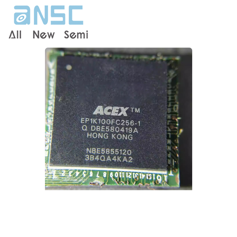
Product Photos


For more product information, please download the PDF