Product Descriptions
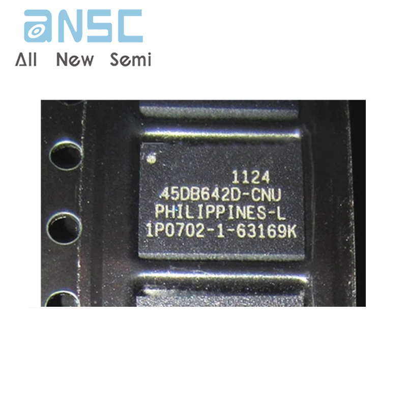
The AT45DB642D is a 2.7-volt, dual-interface sequential access Flash memory ideally suited for a wide variety of digital voice-, image-, program code- and data-storage applications. The AT45DB642D supports RapidS serial interface and Rapid8 8-bit interface. RapidS serial interface is SPI compatible for frequencies up to 66 MHz. The dual-interface allows a dedicated serial interface to be connected to a DSP and a dedicated 8-bit interface to be connected to a microcontroller or vice versa. However, the use of either interface is purely optional. Its 69,206,016 bits of memory are organized as 8,192 pages of 1,024 bytes (binary page size) or 1,056 bytes (standard DataFlash page size) each. In addition to the main memory, the AT45DB642D also contains two SRAM buffers of 1,024 (binary buffer size) bytes/1,056 bytes (standard DataFlash buffer size) each.
The buffers allow receiving of data while a page in the main Memory is being reprogrammed, as well as writing a continuous data stream. EEPROM emulation (bit or byte alterability) is easily handled with a self-contained three step read-modifywrite operation. Unlike conventional Flash memories that are accessed randomly with multiple address lines and a parallel interface, the DataFlash uses either a RapidS serial interface or a 8-bit Rapid8 interface to sequentially access its data.
The simple sequential access dramatically reduces active pin count, facilitates hardware layout, increases system reliability, minimizes switching noise, and reduces package size. The device is optimized for use in many commercial and industrial applications where high-density, low-pin count, low-voltage and low-power are essential.
Product Features
• Single 2.7V - 3.6V Supply
• Dual-interface Architecture
– RapidS™ Serial Interface: 66 MHz Maximum Clock Frequency SPI Compatible Modes 0 and 3
– Rapid8™ 8-bit Interface: 50 MHz Maximum Clock Frequency
• User Configurable Page Size
– 1024 Bytes per Page
– 1056 Bytes per Page
• Page Program Operation
– Intelligent Programming Operation
– 8192 Pages (1024/1056 Bytes/Page) Main Memory
• Flexible Erase Options
– Page Erase (1 Kbyte)
– Block Erase (8 Kbytes)
– Sector Erase (256 Kbytes)
– Chip Erase (64 Mbits)
• Two SRAM Data Buffers (1024/1056 Bytes)
– Allows Receiving of Data while Reprogramming the Flash Array
• Continuous Read Capability through Entire Array
– Ideal for Code Shadowing Applications
• Low-power Dissipation
– 10 mA Active Read Current Typical – Serial Interface
– 10 mA Active Read Current Typical – 8-bit Interface
– 25 µA Standby Current Typical
– 9 µA Deep Power Down Typical
• Hardware and Software Data Protection Features
– Individual Sector
• Permanent Sector Lockdown for Secure Code and Data Storage
– Individual Sector
• Security: 128-byte Security Register
– 64-byte User Programmable Space
– Unique 64-byte Device Identifier
• JEDEC Standard Manufacturer and Device ID Read
• 100,000 Program/Erase Cycles Per Page Minimum
• Data Retention – 20 Years
• Green (Pb/Halide-free/RoHS Compliant) Packaging Options
• Temperature Range
– Industrial: -40°C to +85°C
Product Specifications
| Attribute | Attribute value |
| ANSM-Part# | ANSM-AT45DB642D-CNU |
| Category | Integrated Circuits (ICs) |
| Memory | |
| Memory | |
| Mfr | - |
| Series | - |
| Packaging | Tray |
| Part Status | Obsolete |
| DigiKey Programmable | Not Verified |
| Memory Type | Non-Volatile |
| Memory Format | FLASH |
| Technology | FLASH |
| Memory Size | 64Mbit |
| Memory Organization | 1056 Bytes x 8192 pages |
| Memory Interface | SPI |
| Clock Frequency | 66 MHz |
| Write Cycle Time - Word, Page | 6ms |
| Voltage - Supply | 2.7V ~ 3.6V |
| Operating Temperature | -40°C ~ 85°C (TC) |
| Mounting Type | Surface Mount |
| Package / Case | 8-VDFN |
| Supplier Device Package | 8-CASON (6x8) |
| Base Product Number | AT45DB642 |
Product Photos


For more product information, please download the PDF