Product Descriptions
The Virtex-II family is a platform FPGA developed for high performance from low-density to high-density designs that are based on IP cores and customized modules. The family delivers complete solutions for telecommunication, wireless, networking, video, and DSP applications, including PCI, LVDS, and DDR interfaces.
The leading-edge 0.15 µm / 0.12 µm CMOS 8-layer metal process and the Virtex-II architecture are optimized for high speed with low power consumption. Combining a wide variety of flexible features and a large range of densities up to 10 million system gates, the Virtex-II family enhances programmable logic design capabilities and is a powerful alternative to mask-programmed gates arrays. As shown in Table 1, the Virtex-II family comprises 11 members, ranging from 40K to 8M system gates.
Product Features
• Industry First Platform FPGA Solution
• IP-Immersion Architecture
- Densities from 40K to 8M system gates
- 420 MHz internal clock speed (Advance Data)
- 840+ Mb/s I/O (Advance Data)
• SelectRAM™ Memory Hierarchy
- 3 Mb of dual-port RAM in 18 Kbit block SelectRAM resources
- Up to 1.5 Mb of distributed SelectRAM resources
• High-Performance Interfaces to External Memory
- DRAM interfaces
· SDR / DDR SDRAM
· Network FCRAM
· Reduced Latency DRAM
- SRAM interfaces
· SDR / DDR SRAM
· QDR™ SRAM
- CAM interfaces
• Arithmetic Functions
- Dedicated 18-bit x 18-bit multiplier blocks
- Fast look-ahead carry logic chains
• Flexible Logic Resources
- Up to 93,184 internal registers / latches with Clock Enable
- Up to 93,184 look-up tables (LUTs) or cascadable 16-bit shift registers
- Wide multiplexers and wide-input function support
- Horizontal cascade chain and sum-of-products support
- Internal 3-state bussing
• High-Performance Clock Management Circuitry
- Up to 12 DCM (Digital Clock Manager) modules
· Precise clock de-skew
· Flexible frequency synthesis
· High-resolution phase shifting
- 16 global clock multiplexer buffers
• Active Interconnect Technology
- Fourth generation segmented routing structure
- Predictable, fast routing delay, independent of fanout
• SelectIO™-Ultra Technology
- Up to 1,108 user I/Os
- 19 single-ended and six differential standards
- Programmable sink current (2 mA to 24 mA) per I/O
- Digitally Controlled Impedance (DCI) I/O: on-chip termination resistors for single-ended I/O standards
Product Specifications
| Attribute | Attribute value |
| ANSM-Part# | ANSM-XC2V1000-4FG456C |
| Product Category: | FPGA - Field Programmable Gate Array |
| Series: | XC2V1000 |
| Adaptive Logic Modules - ALMs: | 5120 ALM |
| Embedded Memory: | 720 kbit |
| Number of I/Os: | 324 I/O |
| Supply Voltage - Min: | 1.5 V |
| Supply Voltage - Max: | 1.5 V |
| Minimum Operating Temperature: | 0 C |
| Maximum Operating Temperature: | + 85 C |
| Mounting Style: | SMD/SMT |
| Package / Case: | FBGA-456 |
| Brand: | - |
| Country of Assembly: | Not Available |
| Country of Diffusion: | Not Available |
| Country of Origin: | Not Available |
| Distributed RAM: | 160 kbit |
| Embedded Block RAM - EBR: | 720 kbit |
| Moisture Sensitive: | Yes |
| Number of Gates: | 1000000 |
| Number of Logic Array Blocks - LABs: | 1280 LAB |
| Operating Supply Voltage: | 1.5 V |
| Product Type: | FPGA - Field Programmable Gate Array |
| Subcategory: | Programmable Logic ICs |
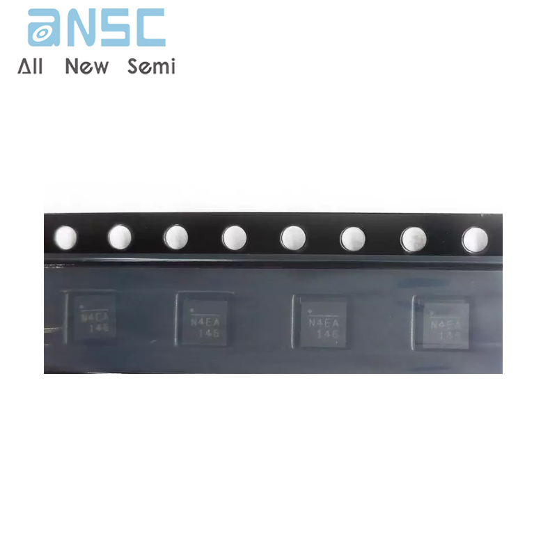
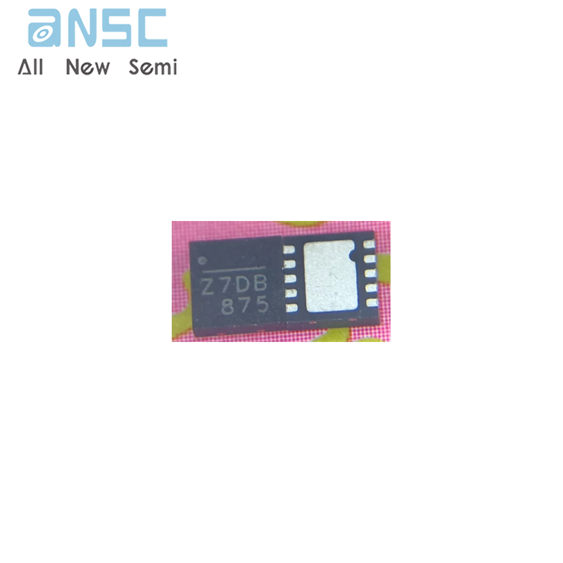
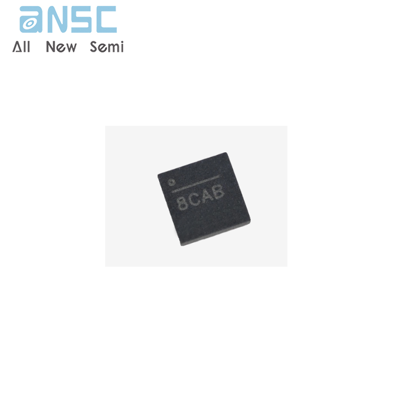
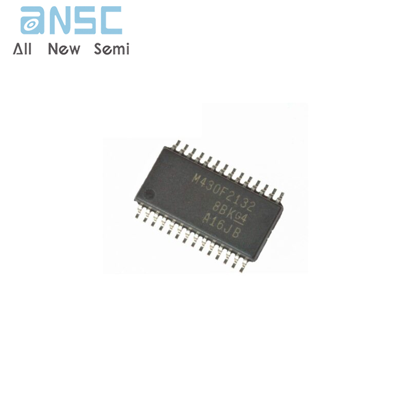
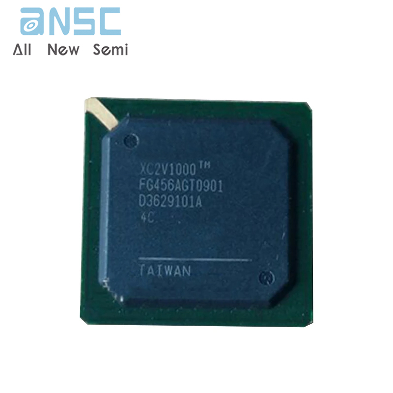
Product Photos


For more product information, please download the PDF