Product Descriptions
The Spartan-II family of FPGAs have a regular, flexible, programmable architecture of Configurable Logic Blocks (CLBs), surrounded by a perimeter of programmable Input/Output Blocks (IOBs). There are four Delay-Locked Loops (DLLs), one at each corner of the die. Two columns of block RAM lie on opposite sides of the die, between the CLBs and the IOB columns. These functional elements are interconnected by a powerful hierarchy of versatile routing channels (see Figure 1).
Spartan-II FPGAs are customized by loading configuration data into internal static memory cells. Unlimited reprogramming cycles are possible with this approach. Stored values in these cells determine logic functions and interconnections implemented in the FPGA. Configuration data can be read from an external serial PROM (master serial mode), or written into the FPGA in slave serial, slave parallel, or Boundary Scan modes.
Spartan-II FPGAs are typically used in high-volume applications where the versatility of a fast programmable solution adds benefits. Spartan-II FPGAs are ideal for shortening product development cycles while offering a cost-effective solution for high volume production.
Spartan-II FPGAs achieve high-performance, low-cost operation through advanced architecture and semiconductor technology. Spartan-II devices provide system clock rates up to 200 MHz. In addition to the conventional benefits of high-volume programmable logic solutions, Spartan-II FPGAs also offer on-chip synchronous single-port and dual-port RAM (block and distributed form), DLL clock drivers, programmable set and reset on all flip-flops, fast carry logic, and many other features.
Product Features
• Second generation ASIC replacement technology
- Densities as high as 5,292 logic cells with up to 200,000 system gates
- Streamlined features based on Virtex® FPGA architecture
- Unlimited reprogrammability
- Very low cost
- Cost-effective 0.18 micron process
• System level features
- SelectRAM™ hierarchical memory:
· 16 bits/LUT distributed RAM
· Configurable 4K bit block RAM
· Fast interfaces to external RAM
- Fully PCI compliant
- Low-power segmented routing architecture
- Full readback ability for verification/observability
- Dedicated carry logic for high-speed arithmetic
- Efficient multiplier support
- Cascade chain for wide-input functions
- Abundant registers/latches with enable, set, reset
- Four dedicated DLLs for advanced clock control
- Four primary low-skew global clock distribution nets
- IEEE 1149.1 compatible boundary scan logic
• Versatile I/O and packaging
- Pb-free package options
- Low-cost packages available in all densities
- Family footprint compatibility in common packages
- 16 high-performance interface standards
- Hot swap Compact PCI friendly
- Zero hold time simplifies system timing
• Core logic powered at 2.5V and I/Os powered at 1.5V, 2.5V, or 3.3V
• Fully supported by powerful Xilinx® ISE® development system
- Fully automatic mapping, placement, and routing
Product Specification
| Attribute | Attribute value |
| ANSM-Part# | ANSM-XC2S150-5FG456C |
| Category | Integrated Circuits (ICs) |
| Embedded | |
| FPGAs (Field Programmable Gate Array) | |
| Mfr | - |
| Series | Spartan®-II |
| Packaging | Tray |
| Part Status | Obsolete |
| DigiKey Programmable | Not Verified |
| Number of LABs/CLBs | 864 |
| Number of Logic Elements/Cells | 3888 |
| Total RAM Bits | 49152 |
| Number of I/O | 260 |
| Number of Gates | 150000 |
| Voltage - Supply | 2.375V ~ 2.625V |
| Mounting Type | Surface Mount |
| Operating Temperature | 0°C ~ 85°C (TJ) |
| Package / Case | 456-BBGA |
| Supplier Device Package | 456-FBGA (23x23) |
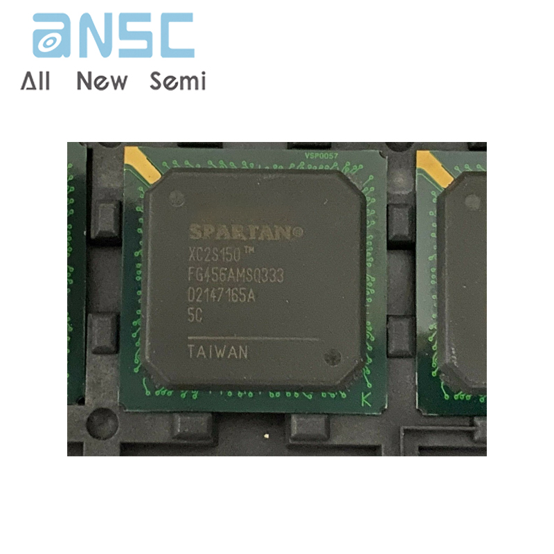
| Base Product Number | XC2S150 |
Product Photos


For more product information, please download the PDF