

Product Descriptions
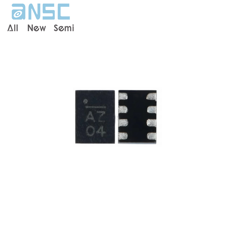
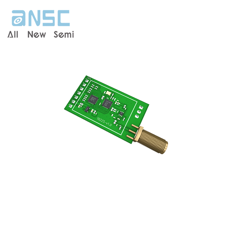
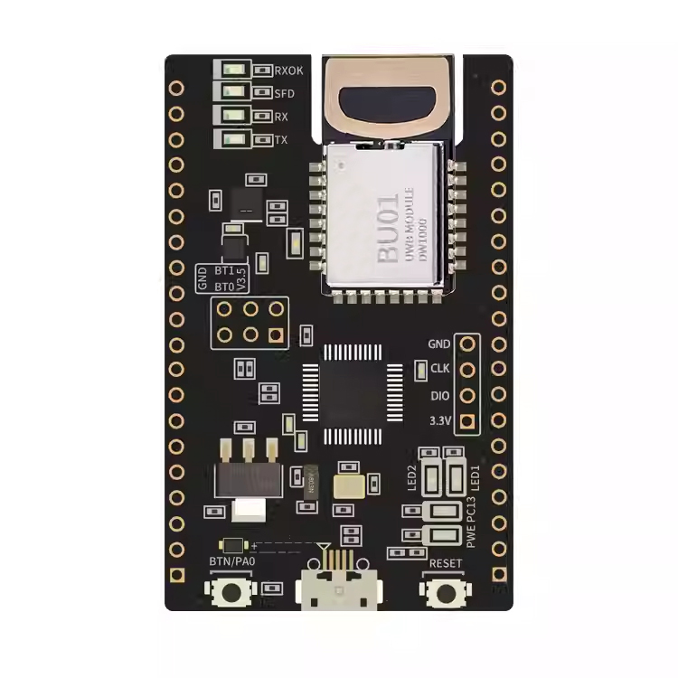
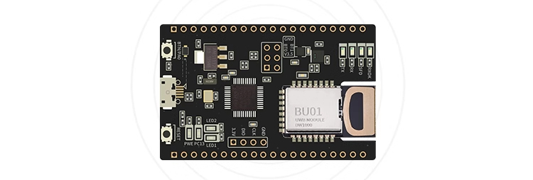
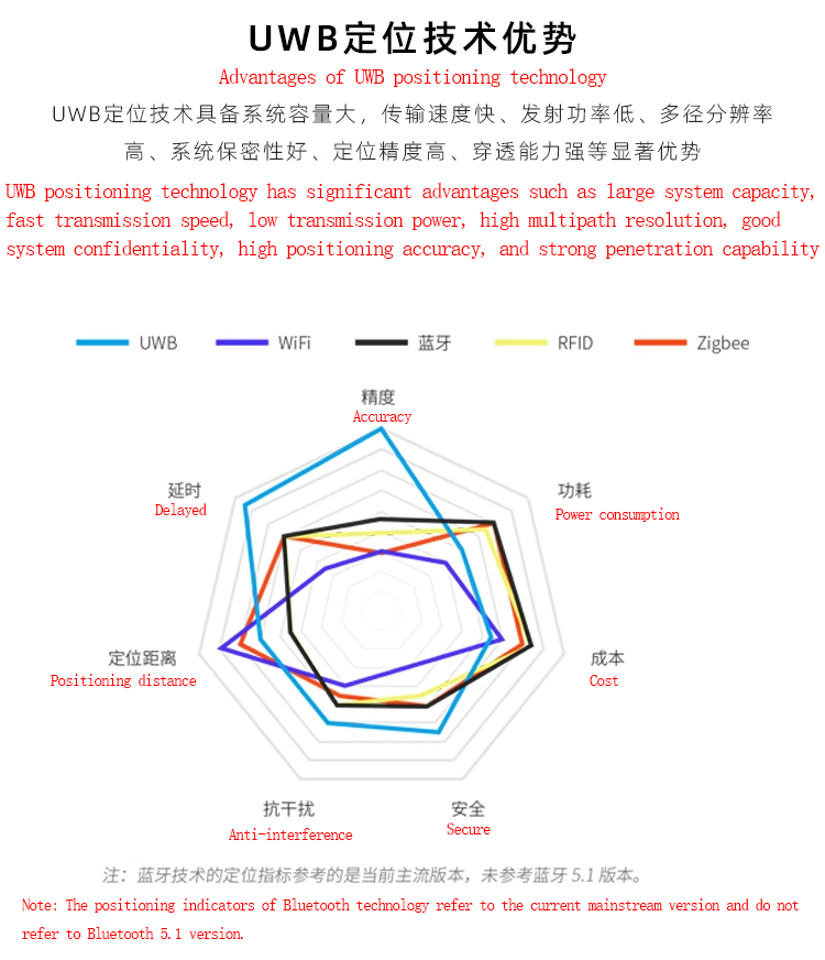
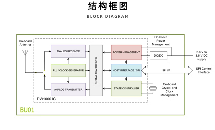
Functional features: Developed based on DecaWave's DW1000 chip, the module integrates antennas, all RF circuits, power management, and clock modules. This module can use bidirectional ranging or TDOA positioning system with a positioning accuracy of 10cm and a data transmission rate of up to 6.8Mbps. It is widely used in nursing homes, parking lots and other fields.
Product Specifications
| 模块型号 Module Type | NodeMCU-BUO1 | 描述 Describe |
| 封装形式 Packaging form | DIP-40 | / |
| 模组尺寸 Module Size | 35*55.5MM | ±0.2mm |
| 协议标准 Protocol standards | IEEE | IEEE 802.15.4-2011 UWB |
| 支持接口 Support interfaces | / | PWM/I2C/GPI0、MCU All IO's |
| 频谱范围 Spectrum range | / | 3.5~6.8GHz |
| 天线形式 Antenna form | 板载 Onboard | 板载PCB天线,传输距离为40米 Onboard PCB antenna with a transmission distance of 40 meters |
| 发射功率 Transmission power | / | 802.11b:16±2dBm;802.11g:16±2dBm;802.11n:16±2dBm; |
| 供电范围 Power supply range | 5V/3.3V | / |
| 工作温度 Operation temperature | 工业级 Industrial grade | -40℃~+85℃ |
Product Pin interface
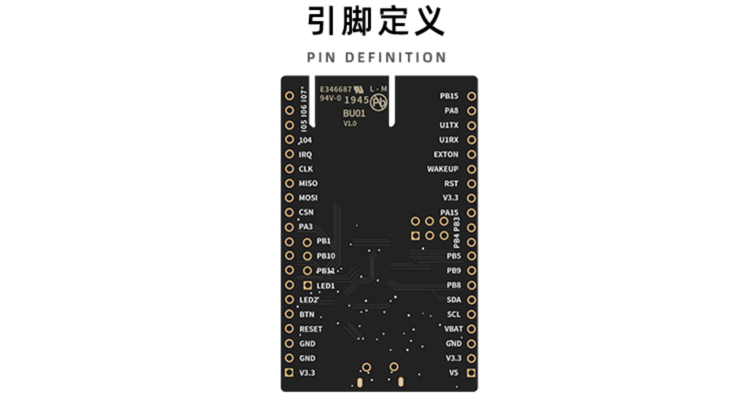
| 脚序 Foot sequence | 名称 Name | 功能说明 Function Description |
| 1 | IO7 | 默认值用作 SYNC 输入。该引脚可以在软件控制下重新配置为通用I/0引脚 GPI07. The default value is used as SYNC input. This pin can be reconfigured as a general-purpose I/O pin GPI07 under software control |
| 2 | IO6 | 通用I/0引脚。上电时,它用作用于配置 SPI 工作模式的 SPIPHA(SPI相位选择)引脚。上电后,该引脚将默认为通用I/0引脚。 Universal I/O pin. When powered on, it is used as the SPIPHA (SPI Phase Select) pin for configuring the SPI operating mode. After power on, this pin will default to the universal I/O pin. |
| 3 | IO5 | 通用I/0引脚。上电时,它用作用于配置 SPI 工作模式的 SPIPOL(SPI 极性选择)引脚。上电后,该引脚将默认为通用I/0引脚。 Universal I/O pin. When powered on, it is used as the SPIPOL (SPI polarity selection) pin for configuring the SPI working mode. After power on, this pin will default to the universal I/O pin. |
| 4 | IO4 | 通用I/0引脚 Universal I/O pin |
| 5 | IRQ | 从 DWM1000 到主机处理器的中断请求输出且与 MCU 的PBO 连接。默认情况下,IRQ是高电平有效输出,但是如果需要,可以将其配置为低电平有效。为了在SLEEP和DEEPSLEEP模式下正确运行,应将其配置为高电平有效运行。该引脚将在休眠和 DEEPSLEEP 状态下浮动,除非将其拉低,否则可能导致伪中断。当不使用IRQ功能时,可以将该引脚重新配置为通用I/0线 GPI08。 Output interrupt requests from DWM1000 to the host processor and connect to the PBO of the MCU. By default, IRQ is a high-level active output, but if necessary, it can be configured to be low-level active. In order to operate correctly in SLEEP and DEEPSLEEP modes, it should be configured for high-level active operation. This pin will float in sleep and DEEPSLEEP states, and unless it is pulled down, it may cause false interrupts. When the IRQ function is not used, the pin can be reconfigured as a general-purpose I/O line GPI08. |
| 6 | CLK | SPI时钟且与 MCU的PA5 连接 SPI clock and PA5 connection with MCU |
| 7 | MISO | SPI数据输出且与MCU的PA6 连接 SPI data output and connected to PA6 of MCU |
| 8 | MOSI | SPI 数据输入且与 MCU的PA7 连接 SPI data input and PA7 connection with MCU |
| 9 | CSN | SPI 芯片选择且与 MCU的PA4 连接。这是一个低电平有效的使能输入。 SPICSn 上从高到低的跳变表示新的SPI事务开始。 SPICSn 还可以用作唤醒信号,使DW1000 退出睡眠或睡眠状态。 Select SPI chip and connect it to PA4 of MCU. This is a low-level active enable input. The transition from high to low on SPICSn indicates the start of a new SPI transaction. SPICSn can also be used as a wake-up signal to cause DW1000 to exit sleep or sleep mode. |
| 10 | PA3 | MCU 上的 PA3 PA3 on MCU |
| 11 | PB1 | MCU 上的 PB1 PB1 on MCU |
| 12 | PB10 | MCU 上的 PB10 PB10 on MCU |
| 13 | PB11 | MCU 上的PB11 PB11 on MCU |
| 14 | LED1 | MCU 上的 PA2,连接LED1 PA2 on MCU, connected to LED1 |
| 15 | LED2 | MCU 上的 PA1,连接 LED2 PA1 on MCU, connected to LED2 |
| 16 | BTN | MCU 上的 PA0,连接 BTN 按键 PA0 on MCU, connect BTN button |
| 17 | RESET | MCU上的复位引脚,连接复位按键 Reset pin on MCU, connected to reset button |
| 18 | GND | 接地 Grounding |
| 19 | GND | 接地 Grounding |
| 20 | 3.3V | 3. 3V 供电 3. 3V power supply |
| 21 | 5V | 5V 供电 5V power supply |
| 22 | 3.3V | 3. 3V 供电 3. 3V power supply |
| 23 | GND | 接地 Grounding |
| 24 | VBAT | MCU 电池电源 Vbat MCU battery power supply Vbat |
| 25 | SCL | MCU 上的 SCL 引脚,默认上拉3.3V,内接传感器SCL脚 SCL pin on MCU, default pull-up 3.3V, internal sensor SCL pin |
| 26 | SDA | MCU 上的 SDA引脚,默认上拉3.3V,内接传感器SDA脚 SDA pin on MCU, default pull-up 3.3V, internal sensor SDA pin |
| 27 | PB8 | MCU 上的 PB8 PB8 on MCU |
| 28 | PB9 | MCU 上的 PB9 PB9 on MCU |
| 29 | PB5 | MCU 上的 PB5 PB5 on MCU |
| 30 | PB4 | MCU 上的PB4 PB4 on MCU |
| 31 | PB3 | MCU 上的 PB3 PB3 on MCU |
| 32 | PA15 | MCU 上的PA15 PA15 on MCU |
| 33 | 3.3V | 3. 3V 供电 3. 3V power supply |
| 34 | RST | BU01上的复位引脚且与MCU的PB12 连接 Reset pin on BU01 and connected to PB12 of MCU |
| 35 | WAKEUP | BU01上的唤醒引脚且与MCU的PB13连接,当置为有效高电平状态时,WAKEUP引脚将 DW1000从休眠或DEEPSLEEP 状态带入工作模式。如果未使用,则该引脚可以接地 The wake-up pin on BU01 is connected to PB13 of the MCU. When set to a valid high state, the WAKEUP pin brings DW1000 from sleep or DEEPSLEEP mode into operation mode. If not used, this pin can be grounded |
| 36 | EXTON | BU01上的 EXTON引脚且与 MCU的PB14 连接,外部设备启用。在唤醒过程中置位并保持活动状态,直到设备进入睡眠模式。可用于控制外部 DC-DC 转换器或设备处于睡眠模式时不需要的其他电路,以最大程度地降低功耗 The EXTON pin on BU01 is connected to the PB14 of the MCU, and the external device is enabled. Set and remain active during the wake-up process until the device enters sleep mode. Can be used to control external DC-DC converters or other circuits that are not needed when the device is in sleep mode, in order to minimize power consumption to the greatest extent possible |
| 37 | U1RX | MCU 上的 UART1-RX UART1-RX on MCU |
| 38 | U1TX | MCU 上的 UART1-TX UART1-TX on MCU |
| 39 | PA8 | MCU 上的PA8 PA8 on MCU |
| 40 | PB15 | MCU 上的PB15 PB15 on MCU |
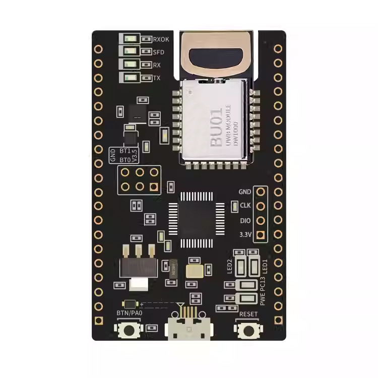
| DIO | Swdio | MCU 上的 SWDI0 脚,默认 MCU 烧录脚 SWDIO pin on MCU, default MCU burning pin |
| CLK | Swclk | MCU 上的 SWDIO 脚,默认 MCU 烧录脚 SWDIO pin on MCU, default MCU burning pin |
| BTO | B00T0 | MCU 上的 BOOT0 脚,控制 MCU 启动方式 BOOT0 pin on MCU, controls MCU startup mode |
| BT1 | B00T1 | MCU 上的 BOOT1 脚,控制 MCU 启动方式 BOOT1 pin on MCU controls MCU startup mode |
| RESET 按键 | RESET | 复位按键 RESET |
| BTN/PA0 按键 | BTN/PA0 | 按下按键拉高PA0 引脚 Press the button to raise the PA0 pin |
Product Show
Payment&Transportation

Official Certificate&Certificate

Multiple product supply

Company office environment

Warehouse Real Shot

Standard packaging

We also provide :
| Part No | Manufacturer | Date Code | Quantity | Description |
| LM22676ADJ | NS | 19+ | 250 | SOP8 |
| TPS562201DDCR | TI | 22+ | 795500 | SOT23-6 |
| NJG1806K75 | JRC | 22+ | 500000 | DFN6 |
| TLV74318PDQNR | TI | 22+ | 402000 | X2SON-4 |
| NJG1801K75 | JRC | 22+ | 300000 | SMD |
| NJG1804K64 | JRC | 22+ | 300000 | DFN8 |
| LM27761DSGR | TI | 22+ | 151000 | WSON8 |
| TLV62565DBVR | TI | 22+ | 138000 | SOT23-5 |
| TPS613222ADBVR | TI | 22+ | 108000 | SOT23-5 |
| LNK625DG-TL | POWER | 22+ | 100000 | SOP-8 |
| OPA4322AIPWR | TI | 22+ | 100000 | TSSOP14 |
| TLV75528PDRVR | TI | 22+ | 99000 | WSON-6 |
| TPS7A2025PDQNR | TI | 22+ | 78500 | X2SON-4 |
| TLV62568DBVR | TI | 22+ | 72000 | SOT23-5 |
| STM32L051K8U6TR | ST | 22+ | 60000 | QFN32 |
| SKY66421-11 | SKYWORKS | 22+ | 56500 | QFN16 |
| TPS7A1111PDRVR | TI | 22+ | 54000 | WSON6 |
| TLV62569PDDCR | TI | 22+ | 52000 | SOT23-6 |
| TLV62569DBVR | TI | 22+ | 48000 | SOT23-5 |
| TPS23753APWR | TI | 22+ | 40000 | TSSOP14 |
| NB691GG-Z | MPS | 22+ | 30000 | QFN |
| SN74AHC1G02DBVR | TI | 22+ | 27939 | SOT-23 |
| TPS63000DRCR | TI | 22+ | 23238 | VSON10 |
| TLV75533PDRVR | TI | 22+ | 21500 | WSON6 |
| NB687BGQ-Z | MPS | 22+ | 20000 | QFN |
| A3916GESTR-T-1 | ALLEGRO | 22+ | 17150 | QFN-20 |
| TPS62135RGXR | TI | 22+ | 15000 | VQFN11 |
| TLE2022AMDR | TI | 0803+ | 12500 | SOP8 |
| TPS23756PWPR | TI | 22+ | 12000 | HTSSOP-20 |