

Product Descriptions
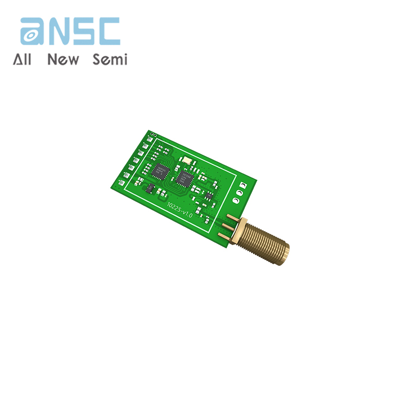
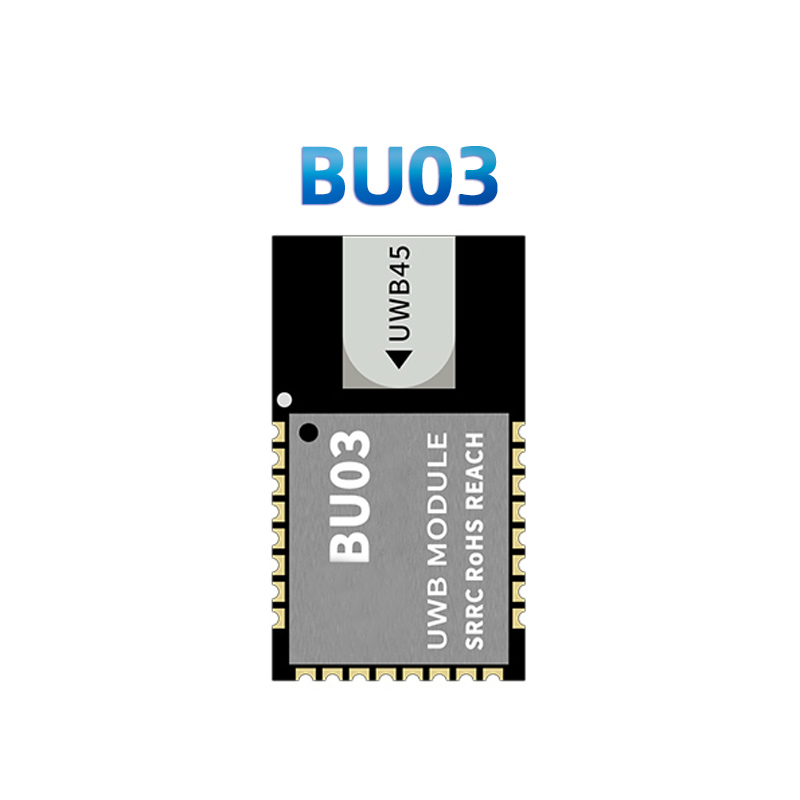
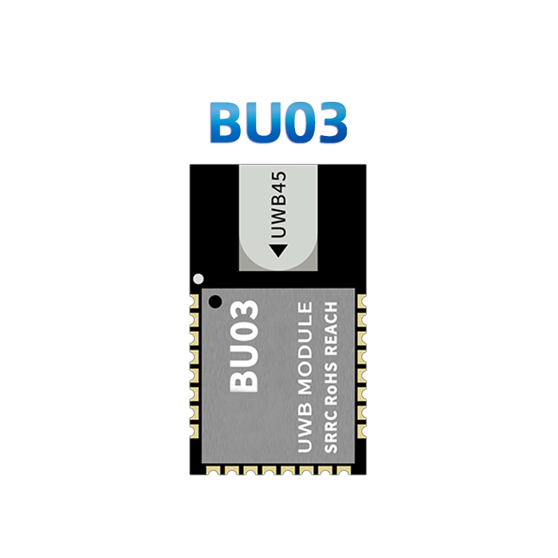
BU03 is an ultra wideband (UWB) module designed based on Decawave's DW3000 series chip. BU03 integrates onboard ceramic antenna, RF circuit, and power management. BU03 can be used in bidirectional ranging, TWR or PDOA positioning systems, with a positioning accuracy of up to 10 centimeters and supporting data rates of up to 6.8 Mbps. It can be widely used in precision positioning, underground coal mine positioning, hospital personnel positioning, warehousing positioning, various indoor positioning and other fields.
Product Specifications
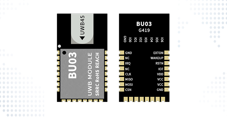
| 模组型号 Module model | BU03 |
| 模组封装 Module packaging | SMD-24 |
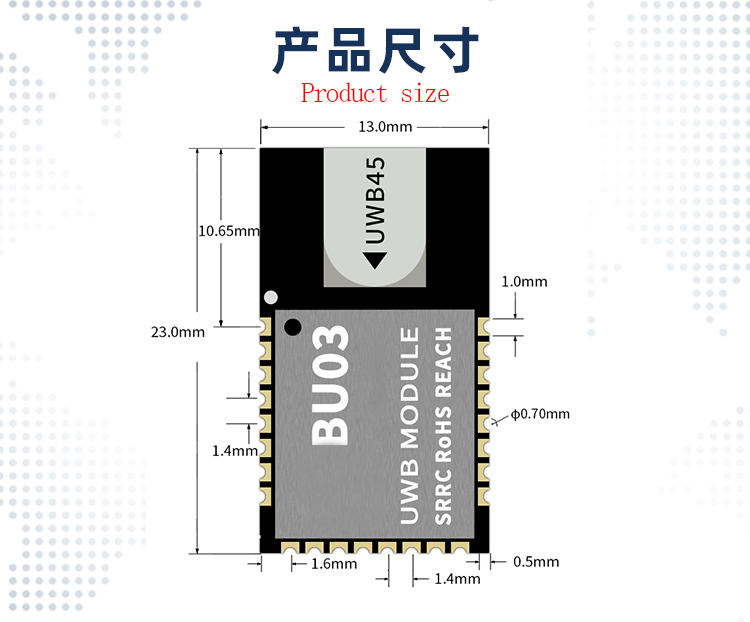
| 尺寸(mm) Size(mm) | 23.0*13.0*2.5(±0.2)MM |
| 天线形式 Antenna form | 板载陶瓷天线 Onboard ceramic antenna |
| 中心频点 Center frequency point | CH5(6489.5MHz)、CH9(7987.2MHz) |
| 工作环境 Work environment | -40℃ ~85℃ |
| 存储环境 Storage environment | -40℃~125°C,<90%RH |
| 供电范围 Power supply range | 供电电压2.5V~3.6V,典型值3.3V。供电电流≥200mA The supply voltage is 2.5V~3.6V, with a typical value of 3.3V. The supply current is ≥ 200mA |
| 支持接口 Support interfaces | SPI |
| 可用IO口数量 Number of available IO ports | 9 |
Module power consumption
The following power consumption data is based on a 3.3V power supply and measured at an ambient temperature of 25 ° C.
| 模式 Mode | 最小值 Minimum value | 平均值 Average value | 最大值 Maximum value | 单位 unit |
| CH5 发射,速率0.85Mbps CH5 transmission, speed 0.85Mbps | - | 18.77 | - | mA |
| CH5 发射,速率6.81Mbps CH5 transmission, speed 6.81Mbps | - | 16.25 | - | mA |
| CH9 发射,速率0.85Mbps CH9 transmission, speed 0.85Mbps | - | 26.43 | - | mA |
| CH9 发射,速率6.81Mbps CH9 transmission, speed 6.81Mbps | - | 24.89 | - | mA |
| CH5 接收,速率0.85Mbps CH5 reception, speed 0.85Mbps | - | 44.17 | - | mA |
| CH5 接收,速率6.81Mbps CH5 reception, speed 6.81Mbps | - | 44.14 | - | mA |
| CH9 接收,速率0.85Mbps CH9 reception, speed 0.85Mbps | - | 53.97 | - | mA |
| CH9 接收,速率6.81Mbps CH9 reception, speed 6.81Mbps | - | 53.74 | - | mA |
| 开机瞬间电流 Instantaneous current during startup | - | 176 | - | mA |
| 深度睡眠 deep sleep | - | 142 | - | mA |
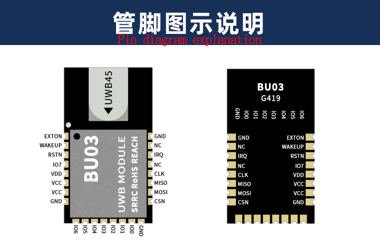
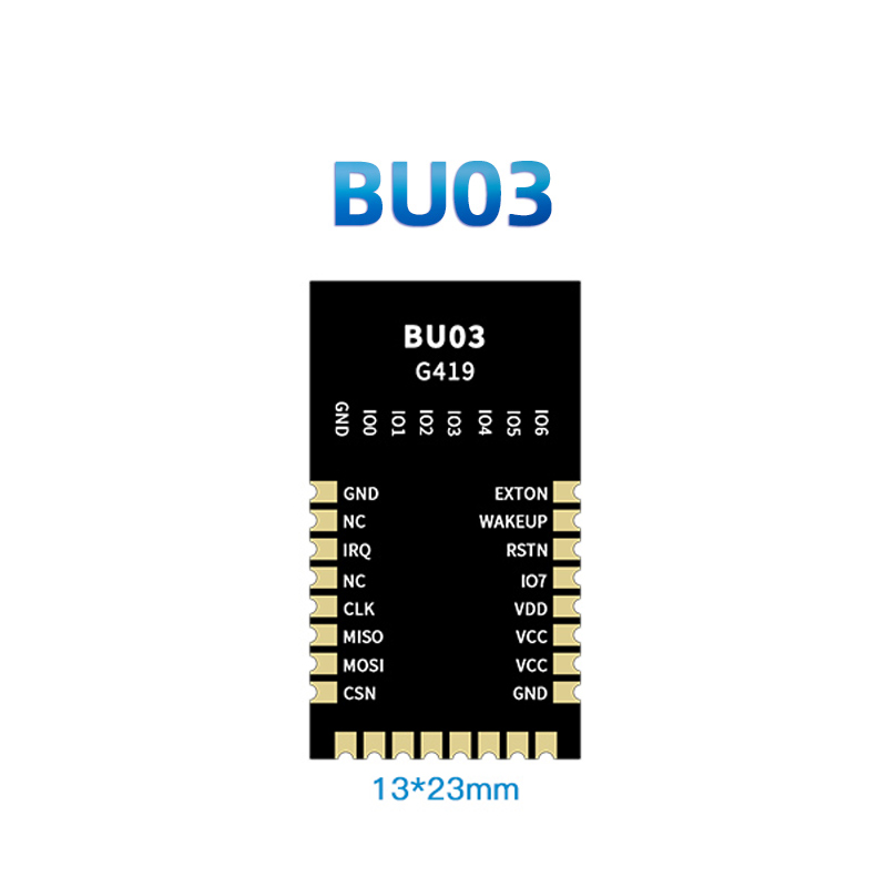
The BU03 module has a total of 24 pins connected, as shown in the pin diagram. The pin function definition table is the interface definition:
| 脚序 Foot sequence | 名称 Name | 功能说明 Function Description |
| 1 | EXTON | 外部设备启用。在唤醒过程中生效,并保持活动状态直到设备进入睡眠模式。可用于控制设备处于睡眠模式时不需要的外部 DC-DC转换器或其他电路,以最大限度地减少功耗 External device enabled. It takes effect during the wake-up process and remains active until the device enters sleep mode. Can be used to control external DC-DC converters or other circuits that are not needed when the device is in sleep mode, in order to minimize power consumption to the greatest extent possible |
| 2 | WAKEUP | 当生效为激活高状态时,WAKEUP引脚将DW3000从睡眠或DEEPSLEEP 状态带入操作模式。如果不使用,应将其接地 When activated to high state, the WAKEUP pin brings DW3000 from sleep or DEEPSLEEP state into operation mode. If not in use, it should be grounded |
| 3 | RSTN | 芯片复位管脚,低电平有效。可由外部开漏驱动器拉低以重置DW3000。不得被外部电源拉高。生效RSTn引脚将完全重置设备,相当于一次电源循环 The chip reset pin is effective at low level. It can be pulled down by an external open drain driver to reset DW3000. Cannot be pulled high by external power sources. The RSTn pin in effect will completely reset the device, equivalent to one power cycle |
| 4 | IO7 | GPIO7/SYNC,SYNC 输入引脚用于外部同步。当不使用SYNC 输入功能时,此引脚可以重新配置为通用 I/O引脚,在内部被拉下 GPIO7/SYNC, the SYNC input pin is used for external synchronization. When not using the SYNC input function, this pin can be reconfigured as a universal I/O pin and pulled down internally |
| 5 | VDD | 电源供电,1.8V~3.6V,外部供电电源输出电流建议在200mA 以上 Power supply, 1.8V~3.6V, external power supply recommended output current above 200mA |
| 6 | VCC | 电源供电,2.5V~3.6V,外部供电电源输出电流建议在200mA 以上 Power supply, 2.5V~3.6V, external power supply recommended output current above 200mA |
| 7 | VCC | 电源供电,2.5V~3.6V,外部供电电源输出电流建议在200mA 以上 Power supply, 2.5V~3.6V, external power supply recommended output current above 200mA |
| 8 | GND | 接地 Grounding |
| 9 | IO6 | GPIO6/EXTRXE/SPIPHA,通用I/O引脚。通电时,它充当SPIPHA(SPI相位选择)引脚,用于配置 SPI操作模式。它可以配置为用作EXTRXE(外部接收器启用)。当DW3000处于接收模式时,此引脚变高。通电后,引脚将默认为通用 I/O引脚 GPIO6/EXTRXE/SPIPHA, Universal I/O pins. When powered on, it serves as the SPIPHA (SPI Phase Select) pin, used to configure the SPI operating mode. It can be configured to be used as EXTRXE (external receiver enabled). When DW3000 is in receive mode, this pin becomes high. After power on, the pins will default to universal I/O pins |
| 10 | IO5 | GPIO5/EXTTXE/SPIPOL,通用I/O引脚。上电时,它充当SPIPOL(SPI极性选择)引脚,用于配置 SPI操作模式。通电后,引脚将默认为通用 I/O引脚。它可以配置为用作EXTTXE(外部传输启用)。当 DW3000 处于传输模式时,此引脚变高 GPIO5/EXTTXE/SPIPOL, Universal I/O pins. When powered on, it serves as the SPIPOL (SPI polarity selection) pin, used to configure the SPI operation mode. After power on, the pins will default to universal I/O pins. It can be configured to be used as EXTTXE (external transmission enabled). When DW3000 is in transmission mode, this pin becomes high |
| 11 | IO4 | GPIO4/EXTPA,通用 I/O引脚。它可以配置为用作EXTPA(外部功率放大器)。此引脚可以启用外部功率放大器 GPIO4/EXTPA, Universal I/O pins. It can be configured to be used as an EXTPA (External Power Amplifier). This pin can enable an external power amplifier |
| 12 | IO3 | GPIO3/TXIED,通用I/O引脚。它可以配置为用作TXLED 驱动引脚,可用于在传输后点亮LED GPIO3/TXIED, Universal I/O pins. It can be configured as a TXLED driver pin, which can be used to light up the LED after transmission |
| 13 | IO2 | GPIO2/TXLED,通用I/O引脚。它可以被配置为用作RXLED 驱动引脚,该驱动引脚可以用于在接收模式期间点亮 LED GPIO2/TXLED, Universal I/O pins. It can be configured to serve as an RXLED driver pin, which can be used to light up the LED during receive mode |
| 14 | IO1 | GPIO1/SFDLED,通用I/O引脚。它可以被配置为用作SFDLED 驱动引脚,当接收器找到 SFD(帧起始分隔符)时,该驱动引脚可以用于点亮 LED GPIO1/SFDLED, Universal I/O pins. It can be configured to be used as an SFDLED driver pin, which can be used to light up the LED when the receiver finds the SFD (frame start delimiter) |
| 15 | IO0 | GPIO0/RXOKLED,通用I/O引脚。它可以被配置为用作RXOKLED驱动引脚,该驱动引脚可以用于在接收到良好帧时点亮 LED GPIO0/RXOKLED, Universal I/O pins. It can be configured to be used as an RXOKLED driver pin, which can be used to light up the LED when a good frame is received |
| 16 | GND | 接地 Grounding |
| 17 | CSN | SPICSn,SPI芯片选择。SPICSn上的高到低转换用信号表示新 SPI事务的开始。SPICSn也可以作为唤醒信号,使DW3000脱离 SLEEP或 DEEPSLEEP 状态 SPICSn, SPI chip selection. The high to low conversion on SPICSn signals the start of a new SPI transaction. SPICSn can also serve as a wake-up signal to disengage DW3000 from SLEEP or DEEPSLEEP state |
| 18 | MOSI | SPI数据输入 SPI data input |
| 19 | MISO | SPI数据输出 SPI data output |
| 20 | CLK | SPI时钟输入 SPI clock input |
| 21 | NC | 悬空管脚 Empty pin |
| 22 | IRQ | GPIO8/IRQ,通用IO引脚。从DW3000到主机处理器的中断请求输出。默认情况下,IQ是有效高输出,但如果需要,可以配置为低有效。为了在 SLEEP 和 DEEPSLEEP 模式下正确操作,应将其配置为主动高有效。该引脚将在 SLEEP 和 DEEPSLEEP 状态下浮动,除非外部拉低(建议 100kΩ),否则可能会在主机上造成虚假中断。当不使用 IRQ 功能时,引脚可以重新配置为通用 IO 线路 GPIO8/IRQ, Universal IO pins. Interrupt request output from DW3000 to the host processor. By default, IQ is effectively high output, but if necessary, it can be configured to be low effective. In order to operate correctly in SLEEP and DEEPSLEEP modes, it should be configured as active high efficiency. This pin will float in SLEEP and DEEPSLEEP states, and unless externally pulled low (recommended 100k Ω), it may cause false interrupts on the host. When the IRQ function is not used, the pins can be reconfigured as universal IO lines |
| 23 | NC | 悬空管脚 Empty pin |
| 24 | GND | 接地 Grounding |
| 注:1、除了 SPICSn外,所有 GPIO 引脚都有一个软件可控的内部下拉电阻器,SPICSn 具有上拉功能,以确保输入引脚未被驱动时的安全操作。内部电阻器的值可随 VDD 电源电压的变化而变化,范围从10kΩ(VDD为1.8V)到30kΩ。 Note: 1. Except for SPICSn, all GPIO pins have a software controllable internal pull-down resistor. SPICSn has a pull-up function to ensure safe operation when the input pin is not driven. The value of the internal resistor can vary with the voltage of the VDD power supply, ranging from 10k Ω (VDD is 1.8V) to 30k Ω. | ||
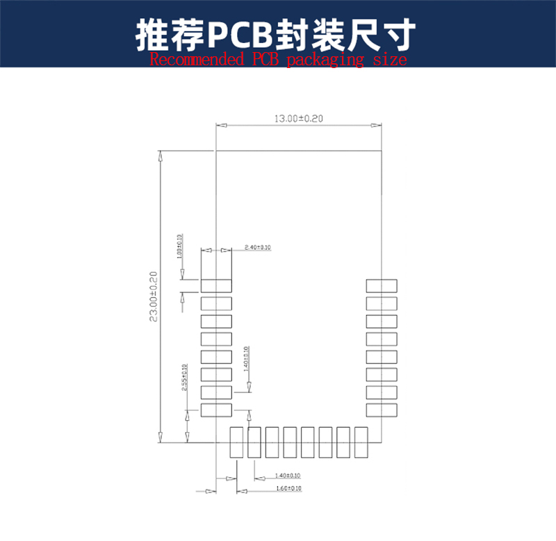
Product Size
Product Show
Payment&Transportation

Official Certificate&Certificate

Multiple product supply

Company office environment

Warehouse Real Shot

Standard packaging

We also provide :
| Part No | Manufacturer | Date Code | Quantity | Description |
| LM22676ADJ | NS | 19+ | 250 | SOP8 |
| TPS562201DDCR | TI | 22+ | 795500 | SOT23-6 |
| NJG1806K75 | JRC | 22+ | 500000 | DFN6 |
| TLV74318PDQNR | TI | 22+ | 402000 | X2SON-4 |
| NJG1801K75 | JRC | 22+ | 300000 | SMD |
| NJG1804K64 | JRC | 22+ | 300000 | DFN8 |
| LM27761DSGR | TI | 22+ | 151000 | WSON8 |
| TLV62565DBVR | TI | 22+ | 138000 | SOT23-5 |
| TPS613222ADBVR | TI | 22+ | 108000 | SOT23-5 |
| LNK625DG-TL | POWER | 22+ | 100000 | SOP-8 |
| OPA4322AIPWR | TI | 22+ | 100000 | TSSOP14 |
| TLV75528PDRVR | TI | 22+ | 99000 | WSON-6 |
| TPS7A2025PDQNR | TI | 22+ | 78500 | X2SON-4 |
| TLV62568DBVR | TI | 22+ | 72000 | SOT23-5 |
| STM32L051K8U6TR | ST | 22+ | 60000 | QFN32 |
| SKY66421-11 | SKYWORKS | 22+ | 56500 | QFN16 |
| TPS7A1111PDRVR | TI | 22+ | 54000 | WSON6 |
| TLV62569PDDCR | TI | 22+ | 52000 | SOT23-6 |
| TLV62569DBVR | TI | 22+ | 48000 | SOT23-5 |
| TPS23753APWR | TI | 22+ | 40000 | TSSOP14 |
| NB691GG-Z | MPS | 22+ | 30000 | QFN |
| SN74AHC1G02DBVR | TI | 22+ | 27939 | SOT-23 |
| TPS63000DRCR | TI | 22+ | 23238 | VSON10 |
| TLV75533PDRVR | TI | 22+ | 21500 | WSON6 |
| NB687BGQ-Z | MPS | 22+ | 20000 | QFN |
| A3916GESTR-T-1 | ALLEGRO | 22+ | 17150 | QFN-20 |
| TPS62135RGXR | TI | 22+ | 15000 | VQFN11 |
| TLE2022AMDR | TI | 0803+ | 12500 | SOP8 |
| TPS23756PWPR | TI | 22+ | 12000 | HTSSOP-20 |