Product Descriptions
The SST49LF008A flash memory devices are designed to be read-compatible with the Intel 82802 Firmware Hub (FWH) device for PC-BIOS application. These devices provide protection for the storage and update of code and data in addition to adding system design flexibility through five general purpose inputs. Two interface modes are supported by the SST49LF008A: Firmware Hub (FWH) Interface mode for in-system programming and Parallel Programming (PP) mode for fast factory programming of PC-BIOS applications.
The SST49LF008A flash memory devices are manufactured with SST’s proprietary, high performance SuperFlash technology. The split-gate cell design and thick-oxide tunneling injector attain better reliability and manufacturability compared with alternate approaches. The SST49LF008A devices significantly improve performance and reliability, while lowering power consumption.
The SST49LF008A devices write (Program or Erase) with a single 3.0-3.6V power supply. They use less energy during Erase and Program than alternative flash memory technologies. The total energy consumed is a function of the applied voltage, current and time of application. Since for any given voltage range, the SuperFlash technology uses less current to program and has a shorter Erase time, the total energy consumed during any Erase or Program operation is less than alternative flash memory technologies. The SST49LF008A products provide a maximum ByteProgram time of 20 µsec. The entire memory can be erased and programmed byte-by-byte typically in 15 seconds when using status detection features such as Toggle Bit or Data# Polling to indicate the completion of Program operation. The SuperFlash technology provides fixed Erase and Program times independent of the number of Erase/ Program cycles performed. Therefore the system software or hardware does not have to be calibrated or correlated to the cumulated number of Erase/Program cycles as is necessary with alternative flash memory technologies, whose Erase and Program time increase with accumulated Erase/ Program cycles.
To protect against inadvertent write, the SST49LF008A devices employ hardware and software data (SDP) protection schemes. It is offered with typical endurance of 100,000 cycles. Data retention is rated at greater than 100 years
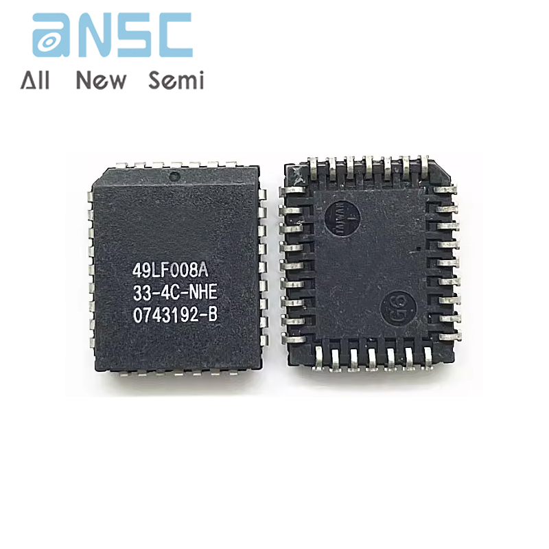
To meet high density, surface mount requirements, the SST49LF008A devices are offered in a 32-lead TSOP package. In addition, the SST49LF008A is offered in 32- lead PLCC and 40-lead TSOP packages. See Figures 2, 3, and 4 for pin assignments and Table 1 for pin descriptions.
Product Features
• Firmware Hub for Intel 8xx Chipsets
• 8 Mbit SuperFlash memory array for code/data storage
– 1024K x8
• Flexible Erase Capability
– Uniform 4 KByte Sectors
– Uniform 64 KByte overlay blocks
– 64 KByte Top Boot Block protection
– Chip-Erase for PP Mode Only
• Single 3.0-3.6V Read and Write Operations
• Superior Reliability
– Endurance:100,000 Cycles (typical)
– Greater than 100 years Data Retention
• Low Power Consumption
– Active Read Current: 6 mA (typical)
– Standby Current: 10 µA (typical)
• Fast Sector-Erase/Byte-Program Operation
– Sector-Erase Time: 18 ms (typical)
– Block-Erase Time: 18 ms (typical)
– Chip-Erase Time: 70 ms (typical)
– Byte-Program Time: 14 µs (typical)
– Chip Rewrite Time: 15 seconds (typical)
– Single-pulse Program or Erase
– Internal timing generation
• Two Operational Modes
– Firmware Hub Interface (FWH) Mode for In-System operation
– Parallel Programming (PP) Mode for fast production programming
• Firmware Hub Hardware Interface Mode
– 5-signal communication interface supporting byte Read and Write
– 33 MHz clock frequency operation
– WP# and TBL# pins provide hardware write protect for entire chip and/or top Boot Block
– Block Locking Register for all blocks
– Standard SDP Command Set
– Data# Polling and Toggle Bit for End-of-Write detection
– 5 GPI pins for system design flexibility
– 4 ID pins for multi-chip selection
• Parallel Programming (PP) Mode
– 11-pin multiplexed address and 8-pin data I/O interface
– Supports fast In-System or PROM programming for manufacturing
• CMOS and PCI I/O Compatibility
• Packages Available
– 32-lead PLCC
– 32-lead TSOP (8mm x 14mm)
– 40-lead TSOP (10mm x 20mm)
– Non-Pb (lead-free) packages available
• All non-Pb (lead-free) devices are RoHS compliant
Product Specifications
| Attribute | Attribute value |
| ANSM-Part# | ANSM-SST49LF008A-33-4C-NHE |
| Category | Integrated Circuits (ICs) |
| Memory | |
| Memory | |
| Mfr | - |
| Series | SST49 |
| Packaging | Tube |
| Part Status | Active |
| DigiKey Programmable | Verified |
| Memory Type | Non-Volatile |
| Memory Format | FLASH |
| Technology | FLASH |
| Memory Size | 8Mbit |
| Memory Organization | 1M x 8 |
| Memory Interface | Parallel |
| Clock Frequency | 33 MHz |
| Write Cycle Time - Word, Page | 20µs |
| Access Time | 120 ns |
| Voltage - Supply | 3V ~ 3.6V |
| Operating Temperature | 0°C ~ 85°C (TA) |
| Mounting Type | Surface Mount |
| Package / Case | 32-LCC (J-Lead) |
| Supplier Device Package | 32-PLCC (11.43x13.97) |
| Base Product Number | SST49LF008 |
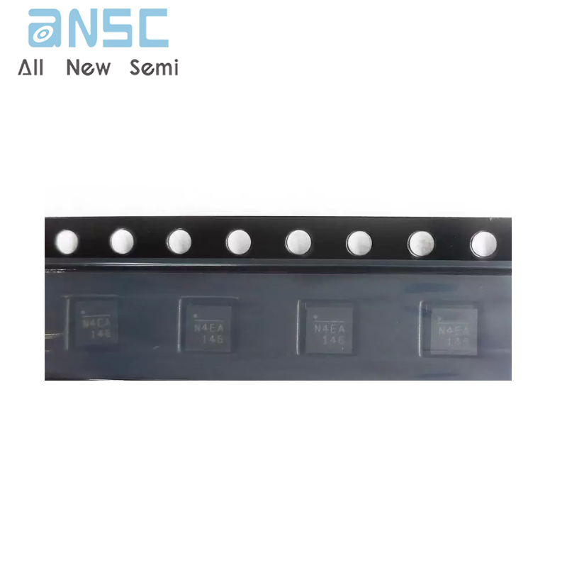
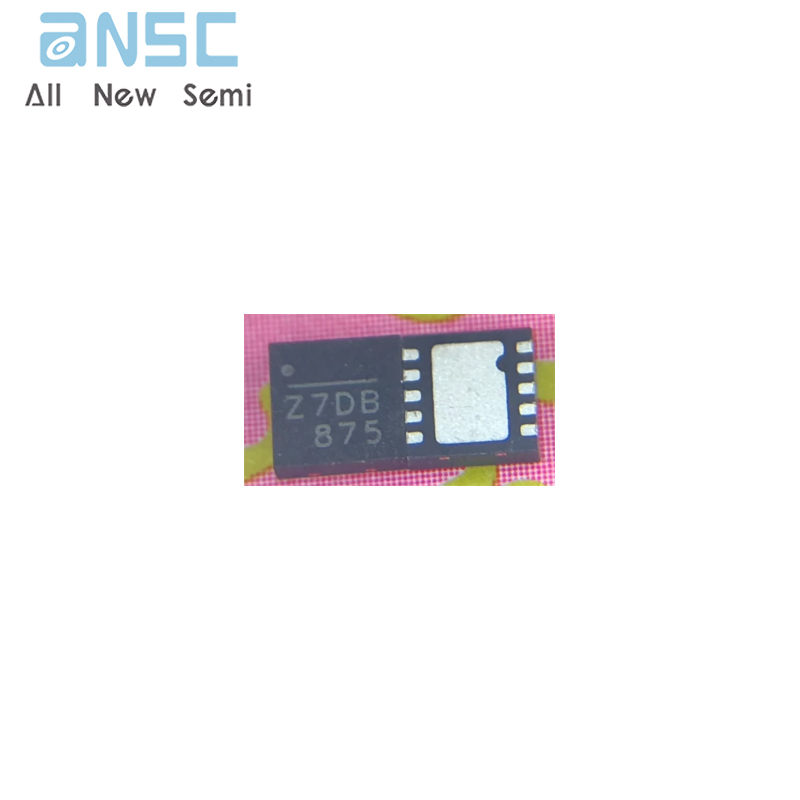
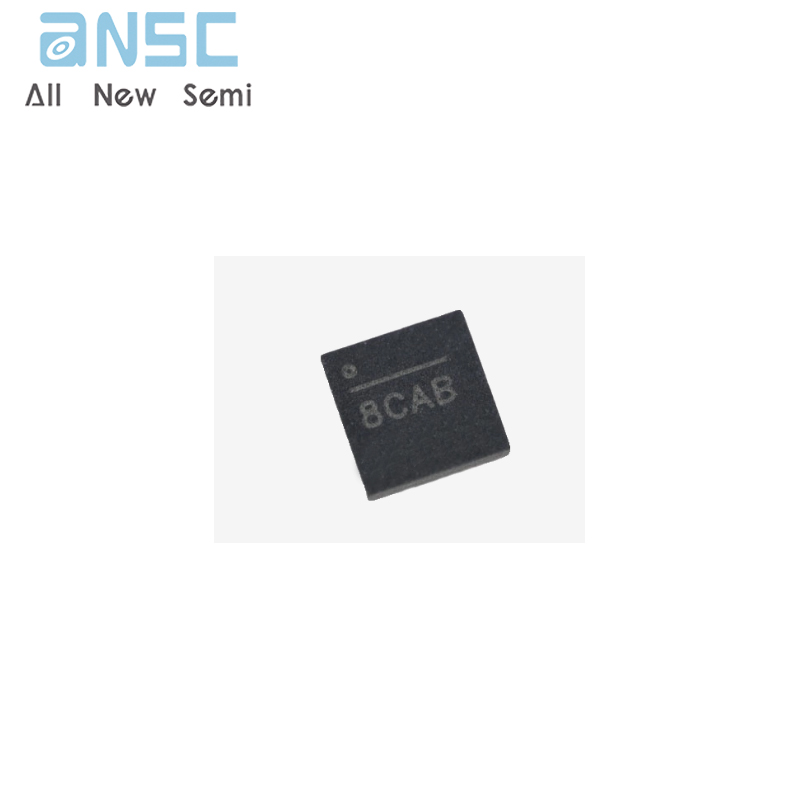
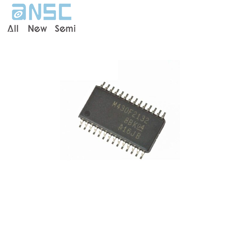
Product Photos


For more product information, please download the PDF