Product Features
• VDD = 2.5V ±0.2V, VDDQ = 2.5V ±0.2V
VDD = 2.6V ±0.1V, VDDQ = 2.6V ±0.1V (DDR400)1
• Bidirectional data strobe (DQS) transmitted/ received with data, i.e., source-synchronous data capture (x16 has two – one per byte)
• Internal, pipelined double-data-rate (DDR) architecture; two data accesses per clock cycle
• Differential clock inputs (CK and CK#)
• Commands entered on each positive CK edge
• DQS edge-aligned with data for READs; centeraligned with data for WRITEs
• DLL to align DQ and DQS transitions with CK
• Four internal banks for concurrent operation
• Data mask (DM) for masking write data (x16 has two – one per byte)
• Programmable burst lengths: 2, 4, or 8
• Auto refresh
– 64ms, 8192-cycle
• Longer-lead TSOP for improved reliability (OCPL)
• 2.5V I/O (SSTL_2 compatible)
• Concurrent auto precharge option is supported
• tRAS lockout supported (tRAP = tRCD)
Product Specifications
| Attribute | Attribute value |
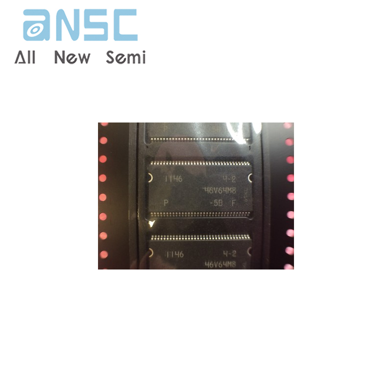
| ANSM-Part# | ANSM-MT46V64M8P-5B:F |
| Category | Integrated Circuits (ICs) |
| Memory | |
| Memory | |
| Mfr | - |
| Series | - |
| Packaging | Tray |
| Part Status | Obsolete |
| DigiKey Programmable | Not Verified |
| Memory Type | Volatile |
| Memory Format | DRAM |
| Technology | SDRAM - DDR |
| Memory Size | 512Mbit |
| Memory Organization | 64M x 8 |
| Memory Interface | Parallel |
| Clock Frequency | 200 MHz |
| Write Cycle Time - Word, Page | 15ns |
| Access Time | 700 ps |
| Voltage - Supply | 2.5V ~ 2.7V |
| Operating Temperature | 0°C ~ 70°C (TA) |
| Mounting Type | Surface Mount |
| Package / Case | 66-TSSOP (0.400", 10.16mm Width) |
| Supplier Device Package | 66-TSOP |
| Base Product Number | MT46V64M8 |
Product Photos

For more product information, please download the PDF