Product Descriptions
The Stratix® II FPGA family is based on a 1.2-V, 90-nm, all-layer copper SRAM process and features a new logic structure that maximizes performance, and enables device densities approaching 180,000 equivalent logic elements (LEs). Stratix II devices offer up to 9 Mbits of on-chip, TriMatrix™ memory for demanding, memory intensive applications and has up to 96 DSP blocks with up to 384 (18-bit × 18-bit) multipliers for efficient implementation of high performance filters and other DSP functions. Various high-speed external memory interfaces are supported, including double data rate (DDR) SDRAM and DDR2 SDRAM, RLDRAM II, quad data rate (QDR) II SRAM, and single data rate (SDR) SDRAM. Stratix II devices support various I/O standards along with support for 1-gigabit per second (Gbps) source synchronous signaling with DPA circuitry. Stratix II devices offer a complete clock management solution with internal clock frequency of up to 550 MHz and up to 12 phase-locked loops (PLLs). Stratix II devices are also the industry’s first FPGAs with the ability to decrypt a configuration bitstream using the Advanced Encryption Standard (AES) algorithm to protect designs.
Product Features
■ 15,600 to 179,400 equivalent LEs; see Table 1–1
■ New and innovative adaptive logic module (ALM), the basic building block of the Stratix II architecture, maximizes performance and resource usage efficiency
■ Up to 9,383,040 RAM bits (1,172,880 bytes) available without reducing logic resources
■ TriMatrixmemory consisting of three RAM block sizes to implement
true dual-port memory and first-in first-out (FIFO) buffers
■ High-speed DSP blocks provide dedicated implementation of multipliers (at up to 450 MHz), multiply-accumulate functions, and finite impulse response (FIR) filters
■ Up to 16 global clocks with 24 clocking resources per device region
■ Clock control blocks support dynamic clock network enable/disable, which allows clock networks to power down to reduce power consumption in user mode
■ Up to 12 PLLs (four enhanced PLLs and eight fast PLLs) per device provide spread spectrum, programmable bandwidth, clock switchover, real-time PLL reconfiguration, and advanced multiplication and phase shifting
■ Support for numerous single-ended and differential I/O standards
■ High-speed differential I/O support with DPA circuitry for 1-Gbps performance
■ Support for high-speed networking and communications bus standards including Parallel RapidIO, SPI-4 Phase 2 (POS-PHY Level 4), HyperTransport™ technology, and SFI-4
■ Support for high-speed external memory, including DDR and DDR2 SDRAM, RLDRAM II, QDR II SRAM, and SDR SDRAM
■ Support for multiple intellectual property megafunctions from MegaCore® functions and Megafunction Partners Program (AMPPSM) megafunctions
■ Support for design security using configuration bitstream encryption
■ Support for remote configuration updates
Product Specifications
| Attribute | Attribute value |
| ANSM-Part# | ANSM-EP2S30F672C5N |
| Category | Integrated Circuits (ICs) |
| Embedded | |
| FPGAs (Field Programmable Gate Array) | |
| Mfr | - |
| Series | Stratix® II |
| Packaging | Tray |
| Part Status | Obsolete |
| DigiKey Programmable | Not Verified |
| Number of LABs/CLBs | 1694 |
| Number of Logic Elements/Cells | 33880 |
| Total RAM Bits | 1369728 |
| Number of I/O | 500 |
| Voltage - Supply | 1.15V ~ 1.25V |
| Mounting Type | Surface Mount |
| Operating Temperature | 0°C ~ 85°C (TJ) |
| Package / Case | 672-BBGA |
| Supplier Device Package | 672-FBGA (27x27) |
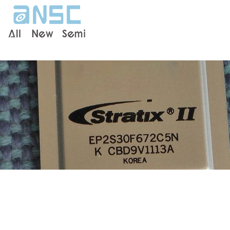
| Base Product Number | EP2S30 |
Product Photos


For more product information, please download the PDF