Product Descriptions
The CY7C2561KV18, CY7C2576KV18, CY7C2563KV18, and CY7C2565KV18 are 1.8V Synchronous Pipelined SRAMs, equipped with QDR-II+ architecture. Similar to QDR-II architecture, QDR-II+ architecture consists of two separate ports: the read port and the write port to access the memory array. The read port has dedicated data outputs to support read operations and the write port has dedicated data inputs to support write operations. QDR-II+ architecture has separate data inputs and data outputs to completely eliminate the need to “turn-around” the data bus that exists with common IO devices. Each port is accessed through a common address bus. Addresses for read and write addresses are latched on alternate rising edges of the input (K) clock. Accesses to the QDR-II+ read and write ports are completely independent of one another. To maximize data throughput, both read and write ports are equipped with DDR interfaces. Each address location is associated with four 8-bit words (CY7C2561KV18), 9-bit words (CY7C2576KV18), 18-bit words (CY7C2563KV18), or 36-bit words (CY7C2565KV18) that burst sequentially into or out of the device. Because data is transferred into and out of the device on every rising edge of both input clocks (K and K), memory bandwidth is maximized while simplifying system design by eliminating bus “turn-arounds”.
These devices have an On-Die Termination feature supported for D[x:0], BWS[x:0], and K/K inputs, which helps eliminate external termination resistors, reduce cost, reduce board area, and simplify board routing.
Depth expansion is accomplished with port selects, which enables each port to operate independently.
All synchronous inputs pass through input registers controlled by the K or K input clocks. All data outputs pass through output registers controlled by the K or K input clocks. Writes are conducted with on-chip synchronous self-timed write circuitry.
Product Features
■ Separate independent read and write data ports
❐ Supports concurrent transactions
■ 550 MHz clock for high bandwidth
■ 4-word burst for reducing address bus frequency
■ Double Data Rate (DDR) interfaces on both read and write ports (data transferred at 1100 MHz) at 550 MHz
■ Available in 2.5 clock cycle latency
■ Two input clocks (K and K) for precise DDR timing
❐ SRAM uses rising edges only
■ Echo clocks (CQ and CQ) simplify data capture in high-speed systems
■ Data valid pin (QVLD) to indicate valid data on the output
■ On-Die Termination (ODT) feature
❐ Supported for D[x:0], BWS[x:0], and K/K inputs
■ Single multiplexed address input bus latches address inputs for read and write ports
■ Separate port selects for depth expansion
■ Synchronous internally self-timed writes
■ QDR™-II+ operates with 2.5 cycle read latency when DOFF is asserted HIGH
■ Operates similar to QDR-I device with 1 cycle read latency when DOFF is asserted LOW
■ Available in x8, x9, x18, and x36 configurations
■ Full data coherency, providing most current data
■ Core VDD = 1.8V± 0.1V; IO VDDQ = 1.4V to VDD [1]
❐ Supports both 1.5V and 1.8V IO supply
■ HSTL inputs and variable drive HSTL output buffers
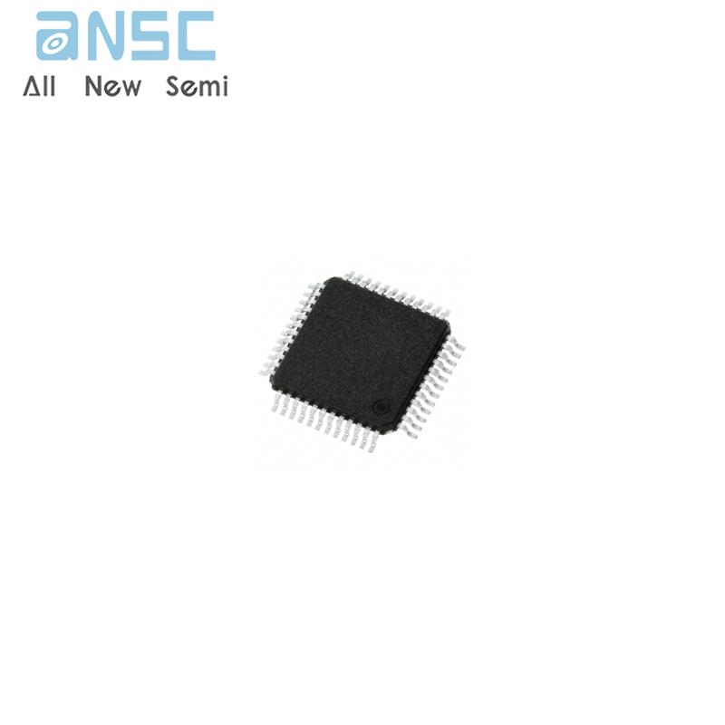
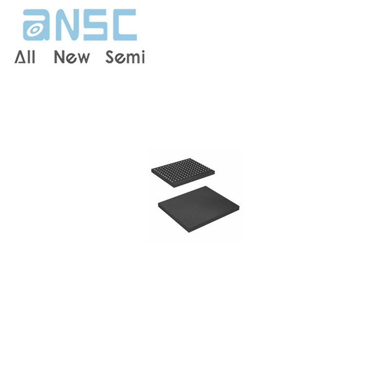
■ Available in 165-Ball FBGA package (13 x 15 x 1.4 mm)
■ Offered in both Pb-free and non Pb-free packages
■ JTAG 1149.1 compatible test access port
■ Phase Locked Loop (PLL) for accurate data placement
Product Specifications
| Attribute | Attribute value |
| ANSM-Part# | ANSM-CY7C2565KV18-400BZXI |
| Category | Integrated Circuits (ICs) |
| Memory | |
| Memory | |
| Mfr | - |
| Series | - |
| Packaging | Tray |
| Part Status | Obsolete |
| DigiKey Programmable | Not Verified |
| Memory Type | Volatile |
| Memory Format | SRAM |
| Technology | SRAM - Synchronous, QDR II+ |
| Memory Size | 72Mbit |
| Memory Organization | 2M x 36 |
| Memory Interface | Parallel |
| Clock Frequency | 400 MHz |
| Write Cycle Time - Word, Page | - |
| Voltage - Supply | 1.7V ~ 1.9V |
| Operating Temperature | -40°C ~ 85°C (TA) |
| Mounting Type | Surface Mount |
| Package / Case | 165-LBGA |
| Supplier Device Package | 165-FBGA (13x15) |
| Base Product Number | CY7C2565 |
Product Photos

For more product information, please download the PDF